Team:Johns Hopkins/Device
From 2010.igem.org
SunPenguin (Talk | contribs) (New page: JHU. <html> <head> <style type="text/css"> #bar-nav { list-style:none; margin:0; padding:0; overflow:hidden; } #bar-nav li { float:left; } #bar-...) |
SunPenguin (Talk | contribs) |
||
| Line 45: | Line 45: | ||
</body> | </body> | ||
</html> | </html> | ||
| + | |||
| + | ==Device Design== | ||
| + | ==='''Microfluidics'''=== | ||
| + | Protocol for creating silicon channels with metal electrodes | ||
| + | <br> | ||
| + | # We grow an oxide mask. The Si wafers are put into an oxidation furnace to grow a layer of SiO2 that’s about 200 nm thick so that it can be used as a mask for the etching of Si in KOH. Water vapor is used to oxidize the Si and the oxidation temperature is 1100 C. <br> | ||
| + | # We then use photolithography to pattern the channels into the silicone wafer. We use a mask and positive resist S1813, coating with a spin at 3500 rpm for a minute to get about 1.2 um layer. Then we bake the wafer at 95C for 2 minutes. The wafer is then exposed to 100mj/cm/cm of UV radiation and then developed in developer CD26 for about a minute. This is followed by a DI water rinse then it is dried. <br> | ||
| + | # We then etch the oxide mask using buffered HF or BOE solutions, in which the etching rate is about 80nm/min. <br> | ||
| + | # The resist is then removed by spraying acetone onto the resist followed by IPA to wash away acetone. <br> | ||
| + | # The fluidic channels are then etched into the Silicone wafer using heated KOH, in which the etching time depends on the desired depth of the channels. The etching rate is about 0.5 micron per minute at 70C. We had etching times of 40 minutes for 20 micron deep channels. <br> | ||
| + | # The remaining oxide is then removed in BOE solution. <br> | ||
| + | # We then grow another layer of oxide on the wafer to electrically isolate the metal electrodes and the substrate.<br> | ||
| + | # We then apply the same photolithography technique described in step 2 to define the electrodes on the wafer. We use mask and a thicker layer of photo resist this time because of the topology of the wafer. <br> | ||
| + | # We then deposit Au on the silicone wafer using an electron beam evaporator. This results in a uniform 100 nm thick layer of Au on the wafer. <br> | ||
| + | # We then remove the resist in acetone then IPA. <br> | ||
| + | # Finally we use photolithography to remove the unwanted oxide, using a third mask. <br> | ||
| + | # A glass slide is then drilled using special ultrahard drill bits, such that the holes are aligned with the inlet and outlet of the microfluidic chip. <br> | ||
| + | # These glass slides are the bonded to the silicone wafer and the device is ready for use. <br> | ||
| + | <br> | ||
| + | The process:<br> | ||
| + | [[Image:Lithography.jpg|center]] | ||
| + | <br> | ||
| + | An overlay of our electrode and channel masks is show below. | ||
| + | <br> | ||
| + | [[Image:Mask.jpeg|300px|center|]] | ||
| + | <br> | ||
| + | 12 Devices are displayed here. Redundancy is important in this process since errors of as little as 5 microns on the aligner, 100rpm when spinning photoresist, or a few seconds in etching solution could easily render a device unusable. There are 2 devices with 300 micron channels (easiest to make), 4 with 200 micron channels (lower odds of success requires more redundancy), and 6 with 100 micron channels (extremely difficult to make). In fact, none of the 100 micron channels worked. In our process, the photoresist that determines the electrode positions is applied to a wafer with channels already present. Since light diffracts if there is any distance between mask and substrate, the size of features pattered at the bottom of channels is distorted. Thus, our electrodes, which were supposed to take the form of two separate columns on either side of the channel, fused across the 100 micron space. | ||
Revision as of 22:51, 27 October 2010
Device Design
Microfluidics
Protocol for creating silicon channels with metal electrodes
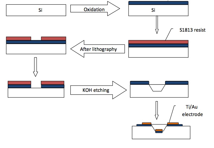
- We grow an oxide mask. The Si wafers are put into an oxidation furnace to grow a layer of SiO2 that’s about 200 nm thick so that it can be used as a mask for the etching of Si in KOH. Water vapor is used to oxidize the Si and the oxidation temperature is 1100 C.
- We then use photolithography to pattern the channels into the silicone wafer. We use a mask and positive resist S1813, coating with a spin at 3500 rpm for a minute to get about 1.2 um layer. Then we bake the wafer at 95C for 2 minutes. The wafer is then exposed to 100mj/cm/cm of UV radiation and then developed in developer CD26 for about a minute. This is followed by a DI water rinse then it is dried.
- We then etch the oxide mask using buffered HF or BOE solutions, in which the etching rate is about 80nm/min.
- The resist is then removed by spraying acetone onto the resist followed by IPA to wash away acetone.
- The fluidic channels are then etched into the Silicone wafer using heated KOH, in which the etching time depends on the desired depth of the channels. The etching rate is about 0.5 micron per minute at 70C. We had etching times of 40 minutes for 20 micron deep channels.
- The remaining oxide is then removed in BOE solution.
- We then grow another layer of oxide on the wafer to electrically isolate the metal electrodes and the substrate.
- We then apply the same photolithography technique described in step 2 to define the electrodes on the wafer. We use mask and a thicker layer of photo resist this time because of the topology of the wafer.
- We then deposit Au on the silicone wafer using an electron beam evaporator. This results in a uniform 100 nm thick layer of Au on the wafer.
- We then remove the resist in acetone then IPA.
- Finally we use photolithography to remove the unwanted oxide, using a third mask.
- A glass slide is then drilled using special ultrahard drill bits, such that the holes are aligned with the inlet and outlet of the microfluidic chip.
- These glass slides are the bonded to the silicone wafer and the device is ready for use.
The process:
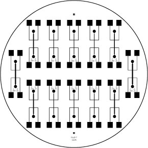
An overlay of our electrode and channel masks is show below.
12 Devices are displayed here. Redundancy is important in this process since errors of as little as 5 microns on the aligner, 100rpm when spinning photoresist, or a few seconds in etching solution could easily render a device unusable. There are 2 devices with 300 micron channels (easiest to make), 4 with 200 micron channels (lower odds of success requires more redundancy), and 6 with 100 micron channels (extremely difficult to make). In fact, none of the 100 micron channels worked. In our process, the photoresist that determines the electrode positions is applied to a wafer with channels already present. Since light diffracts if there is any distance between mask and substrate, the size of features pattered at the bottom of channels is distorted. Thus, our electrodes, which were supposed to take the form of two separate columns on either side of the channel, fused across the 100 micron space.
 "
"


